DIAG264
Diag264 © 2021 by Rob Clarke is licensed
under CC BY-NC-ND 4.0
Important message
|
Dear Diag264
users,
I hope you
enjoy Diag264 and find it useful. Diag264 is now licensed under a Creative
Commons Attribution-NonCommercial-NoDerivatives 4.0 International License,
otherwise known as CC BY-NC-ND 4.0. This means it is free to download and
distribute the unmodified Diag264 software for personal use, but it must
include a link to the Diag264 website, and the license (Attribution). It is
not permitted to modify and then distribute the software (NoDerivatives), and
neither is it permitted to resell the software in any form (NonCommercial).
The reason
I've done this is to enable me to continue to provide free support to users
from code I know. Over the 10 years since I first released Diag264, I get 2
or 3 mails per month to the Diag264 email address asking for help with fixing
the issues and interpreting the results, which I'm always willing to do
within the constraints of my free time, plus it helps me improve future
releases.
Until now
I've never had any license restrictions, which has meant a number of
resellers have started selling it on Ebay or via their own web-shops. Some
have asked permission beforehand, but most didn't. In late 2020 I spent some
days trying to help someone with their C16 before we figured out that he was
using a version of Diag264 that had been modified and broken in the process. While
looking into this I then found another reseller had appeared on Ebay claiming
the work as his own and having removed my name. Hopefully you can all
understand how frustrating this is.
If you want
the software, you can download it and burn it to an EPROM/PROM yourself or,
if you don't have access to an EPROM burner, I will sell you pre-programmed
for cost of postage and the cost of the EPROM only. Please send me a message
you would like this.
I will allow
resale of the dongles and loop backs, as long as the attribution conditions
are met as described above.
If you did
purchase this software from another seller, I would encourage you to let me
know the details by emailing me at diag264@inchocks.co.uk, as
it’s against the terms of the license and discourages me from further
development and support of Diag264.
Regards, Rob
|
Introduction
DOWNLOAD
HERE!
This document describes operation of the Diag264 diagnostic
tool and harness. It can be used to assist in the identification of faults with
RAM, ROM, I/O & CPU ports, and TED registers. It has been tested on a wide
range of 264 series (aka TED) machines, including some non-standard
configurations and PAL and NTSC machines. This includes the C116, Commodore 16,
C232 and Plus/4, and even a V364!
Credits
It was developed primarily on a Windows 7 PC using TextPad, 64Tass,
YAPE and
VICE.
Thank you, in no particular order, to the following:
·
Bil Herd,
the lead engineer of the TED project, and who also wrote the TED
System Hardware Manual, Terry Ryan, Fred Bowen, John Cooper, Dave
Haynie, Bruce Ahearns, Dave DiOrio, Eric Yang, Bob Olah, Ted Lengthy and
countless other Commodore engineers who designed the chips and engineered the
TED system and to whoever in this list who wrote the 7360
Data Sheet !
·
Hársfalvi Levente (TLC) for thoughts on cold starting from
cartridges, joystick ports & TED latches
·
Martin Korth for the pagezero commodore specifications
·
Valentino Zenari (SVS) for the most excellent SVS ROM Map
·
Attila Grósz (Gaia) for the extremely cool YAPE
emulator.
·
Groepaz and the
Vice team for the equally cool VICE emulator and fixing the
bugs within days!
·
The Western Design Center for information on the 6551.
- Csaba Pankaczy (csabo) for info on which TED registers to
check.
- SukkoPera for the OpenC16Cart
project, saving countless original cartridges for their original purpose.
The HTML version of the
document can be found here and you can
contact me either by a private message to ‘crock’ on Plus4World or Lemon64.
You can also send email to a filtered email account at 
Disclaimer
As soon as you undo the screws
and lift up the lid on an old 8-bit machine, there is an element of risk
involved. To use this diagnostic tool in its most effective form, it requires
replacing the kernel ROM in the machine and attaching loop-back connectors to
the interface ports. The TED chip especially is sensitive to abuse and the
built in latch register is easily broken by stray voltages and static.
Although I describe how to
build such connectors that I have successfully used myself, they are not
required to test the keyboard and joysticks if you don’t need to run the tests
unattended. Diag264 does provide features to manually test the keyboard and
joysticks and to bypass them to allow the rest of the tests to run unattended.
As keyboard and joystick problems are not usually intermittent in nature, this should
not be an issue for most users.
If you do choose to build loop-back
connectors for the keyboard or joysticks, I will provide any guidance that I
can, but please understand that you do so at your own risk.
Background
I acquired or built most of
Commodore's official diagnostic cartridges and harnesses for the 64, VIC-20 and
C128, which they sold to service centres, mainly to help me fix the growing
pile of computers I’d acquired. Fixing them became somewhat an obsessive-compulsive
habit, and I could not bear having broken machines lying around. In amongst
them I had a C16 and two Plus/4’s, only one of which worked. I started
searching around for a diagnostic cartridge for the 264 series but with no
luck. I knew Commodore had definitely made one, but I could not track it down. Finally,
I found an image of one on Plus4World, but as I never
got any response from the owner, I decided that my only choice was to build my
own.
Design and Theory of Operation
The design and operation of
Diag264 is closely modelled on the operation of the cartridges available for
the 64/128 and VIC-20. One of the aspects that I was most keen to copy was the
functionality of the Dead Test Cartridge of the 64. The primary use of this
cartridge was to find RAM issues in a machine that otherwise appeared dead.
The majority of Commodores
later 8-bit offerings used DRAM chips in either a 64k x 1 or 16k x 4
configuration. This usually meant that any dead RAM chip would make the machine
completely inoperable, as the zero page ($0002-$00FF) and stack ($0100-$01FF)
are rendered practically unusable. The kernal start-up routines in both the 64
and 264's make extensive use of the ZP and implicitly rely on the stack upon
the first execution of an RTS instruction. This presents a problem for any
normal cartridge based diagnostic tool because we are dependent on the kernal
to hand over control to the cartridge ROM.
The Dead Test cartridge avoids
this problem by making use of the 64's Ultimax mode, which was a legacy from
the MAX Machine, a cartridge only based console system which was a subset of
the later 64’s architecture. The Ultimax compatibility mode enables an external
cartridge ROM to replace the Kernal of the host machine and therefore bypass
the normal start-up routines, making it ideal for identifying RAM problems on
an otherwise ‘dead’ system.
The 264 architecture does not
include any way of auto-booting into an external ROM without trying to pull
some dirty tricks with the address lines, so it becomes a trade-off between the
conveniences of a cartridge versus the extra benefits of booting straight into
the diagnostic. The Diag264 ROM can therefore be compiled for either cartridge
or kernal.
The kernal option is a drop in
replacement of the kernal ROM, which is the 28-pin ROM chip with the identifier
beginning with 318004 (PAL) or 318005 (NTSC), which is in location U4 in a C16
and C116, and U24 in a Plus/4.
The cartridge, or low-ROM,
option involves either sacrificing a standard commercial Commodore C16/Plus
cartridge or, preferably, you can acquire a SukoPerra designed 264
cartridge blank from PCBWay.
The cartridge version is also known as the low-ROM option because it will work
in any of the available sockets which map to the low block of ROM from $8000 to
$C000. This means the low-ROM version will also work in the BASIC ROM socket
(U23 in a Plus/4, U3 in a C16/C116), and the low function ROM socket (U25 in a
Plus/4, not present in a C16/C116.)
If you choose to modify an existing
cartridge, you will need to remove the ‘low’ ROM and install a 28-pin DIL socket
in its place. With the edge connector facing towards you, this is the socket on
the left. The image in Figure 1, which is my own cartridge, also has a socket
in the ‘high’ ROM position, on the right. This is not required for Diag264.
Figure 1 - Cartridge Mod
The TED chip itself supports both NTSC and PAL standards, controlled
by bit 6 of register $FF07. The only differences between NTSC and PAL machines are
a different clock crystal and a slightly different kernal to correctly set the
state of the PAL/NTSC bit, and some other small modifications to take into
account timing differences.
When running from a cartridge or any of the low-ROM sockets, Diag264
queries the installed kernal to determine whether it should set NTSC or PAL
mode by checking the value of $F33F, which contains the default value for TED
register $FF07. The kernal version has no way to determine from software
whether the base machine is NTSC or PAL, so the ROM image is available in
versions which default to either NTSC or PAL. Nevertheless, for both the
cartridge and kernal options, it is possible to override the default by holding
down ‘P’ or ‘N’, as the machine is powered on, to force the software into PAL
or NTSC respectively.
Loop-back connectors
To determine the correct
operation of the various I/O interfaces, a number of loop-back connectors are
required. For a C16 or C116 you need a minimum of a serial port and cassette
connector. For a Plus/4 an additional user port loop-back is required to test
the Asynchronous Communications Interface Adapter (ACIA) interface and the 6529
8-bit port. The ACIA is a 6551/8551 chip which provides the RS232 support via
the user port.
It is also possible to
construct connectors for the joystick ports and keyboard, but this is not an
absolute requirement if the user is prepared to manually execute the keyboard and
joystick tests.
Cassette Connector
The cassette connector requires
a 7 pin mini-din connector, two 330 ohm resistors and a few short lengths of
wire. The diagram below is viewed looking at the rear/solder side of the plug.
|

Figure 2
- Cassette Connector
|
1.
GND
2.
+5v
3.
Motor
4.
Read
5.
Write
6.
Sense
7.
GND
|
The read line [4] is directly
connected to the write line [5] while the two resistors form a voltage divider
between the motor [3] and GND[7], with the resulting output being sufficient to
pull the sense [6] line high when the cassette motor is activated.
7 pin mini-din plugs can be
sourced from most electronics retailers such as Digikey or Mouser, and are
plentiful on Ebay. They can be rather tricky to solder given the small pitch of
the pins. It may be easier to find another lead with a 7-pin moulded plug
pre-attached if you happen to have one to hand.
Serial Connector
The serial connector is very
simple. As the data and clock lines are bi-directional, they are internally
looped back, the only exception being the ATN line. The connector consists of a
single link between the ATN [3] and Clock [4] line. The diagram below is viewed
looking at the rear/solder side of the plug.
|
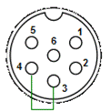
Figure 3
- Serial Connector
|
1. N/C (Plus/4 & C232), +5v (C16 & C116)
2. GND
3. ATN
(Out)
4. Clock
(In/Out)
5. Data
(In/Out)
6. Reset
|
6 pin DIN plugs are in
plentiful supply and easy to solder as they usually have cups to hold the wire.
User Port Connector (plus/4 Only)
The User Port connector serves
two purposes, firstly to test the 8-bit 6529 port, and secondly the 6551/8551 ACIA
RS232 interface. This is constructed using a 24-way edge connector with .156”
spacing, the same as found on other Commodore 8 bit machines. The diagram below
is viewed from the rear of the plug. This connector can be acquired from the
sources mentioned above as well as from Jim Brain’s
go4retro store.
You need to make seven links,
four linking ports 0-3 on the 6529 to ports 4-7, which requires joining [B]
-> [6], [K] -> [7], [4] -> [J] and [5] -> [F] respectively. Then three
connections looping back the signals for the ACIA. These are [C] -> [M], [D]
-> [L] and [E] -> [H]. This implements a standard RS232 loop-back, the
only difference being that the plus/4 does not expose CTS on the user port.
Further detail about RS232 loop-backs can be found in the datasheet for the
equivalent W65C51N from the Western Design Center. (W65C51N
Datasheet)
Ensure that you clearly label
your connector ‘top’ and ‘bottom’ or preferably, insert the vertical keys
between 1 & 2 and A & B then 10 & 11 and L & M, as shown by
the blue dotted lines in the diagram. If you insert it upside down, you will short
the 9V AC to the 5V DC line and you will likely destroy something in your
machine.

Figure 4 - User Port Connector
|
1.
GND
2.
+5V
3.
/BRESET - Buffered Reset
4.
6529 – P2 (also Cassette Sense)
5.
6529 – P3
6.
6529 – P4
7.
6529 – P5
8.
RxC – Receive Clock
9.
ATN – IEC Attention
10. 9V
AC
11. 9V
AC
12. GND
|
A.
GND
B.
6529 – P0
C.
RxD – Receive Data
D.
RTS – Request to Send
E.
DTR – Data Terminal Ready
F.
6529 – P7
H.
DCD – Data Carrier Detect
J.
6529 – P6
K.
6529 – P1
L.
DSR – Data Set Ready
M. TxD
– Transmit Data
N.
GND
|
Table 1
- User Port Pin Description
Keyboard loop-back
There are two types of connector used on the 264 series. The
easy one is for the C16, which uses the same style keyboard connector as the
VIC-20/C64, albeit with a different layout, and uses a 20-pin SIL (single
in-line) plug with a 0.1” (2.54mm) pitch.
This plug can be built using a 40-pin IDE cable from a PC hard
drive which has the same 0.1” pitch. 80-pin IDE cables have each alternate
conductor grounded to reduce crosstalk but the wires are finer and difficult to
work with, so you’re better off avoiding them. Peter Schepers has some info on
preparing a similar plug for a Commodore 64 diagnostic harness here http://ist.uwaterloo.ca/~schepers/diagnostic.html.
The process is to split out the odd numbered wires and cut the rest back close
to the plug. Pin 1 is usually marked by a different colour.
The wires need to be connected as shown in Figure
5 and Table 2 - Keyboard Signals. Pins 2, 4, 5 & 20 of the keyboard
connector (not the IDE numbering) have no connection and pin 2 is used as a
key. I blocked off pin 2 with a pin from another header plug. As the other side
of the IDE cable has pin 20 blocked off, this makes it impossible to connect
the plug incorrectly. The contacts on a typical keyboard have around 110 ohms
of resistance, so I suggest putting small resistors in line to limit the
current. There is also a small signal diode with the cathode connected to the
keyport 6529 (Signal Out) side of the connector to prevent the joystick loop-back
interfering with the testing of the keyport.

Figure
5 - C16 Keyboard connector
The C116 and Plus/4 use an 18-way FFC (Flat Flexible Cable)
connector. Although the mechanical construction of the keyboard for the Plus/4
and C116 is quite different, it is electrically compatible, so you can use a
Plus/4 keyboard on a C116 and vice-versa.
This connector is not easy to construct unless you have a
supply of 18-way FFC cables. Some have had success using 0.1 inch pin headers,
but my concern with this approach is that the pins are much thicker than the
cable and it may stress the socket to the point where the original cable does
not make a good electrical connection. The other common issue is that as the
machines get older, the ends of the FFC cable have a habit of delaminating,
meaning the metal separates from the plastic making it a challenge to insert
the FFC into the socket. I would recommend that for casual use, the user just
stick with manual testing of the keyboard. The pins are in the same order but
numbered differently on the C116 and Plus/4, as seen in columns 6 and 7 of Table 2 - Keyboard Signals.
|
Signal Out
|
Signal In
|
Key
|
C16 Pin Out
|
C16 Pin In
|
Plus/4, C116 Pin Out
|
Plus/4, C116 Pin In
|
|
D0
|
K4
|
F1
|
19
|
7
|
18
|
6
|
|
|
D1
|
K5
|
S
|
8
|
9
|
7
|
8
|
|
|
D2
|
K6
|
T
|
12
|
10
|
11
|
9
|
|
|
D3
|
K7
|
V
|
11
|
3
|
10
|
2
|
|
|
D4
|
K0
|
9
|
13
|
18
|
12
|
17
|
|
|
D5
|
K1
|
P
|
1
|
15
|
1
|
14
|
|
|
D6
|
K2
|
;
|
16
|
14
|
15
|
13
|
|
|
D7
|
K3
|
2
|
6
|
17
|
5
|
16
|
|
Table
2 - Keyboard Signals
Joystick loop-back
The design of the joystick interface on the 264 series is
different to other 8-bit Commodore computers. With the exception of the fire
buttons, all the control lines from ports 1 and 2 are all wired together and
connected to the TED’s keyboard latch. Whereas the 64’s joystick interface
worked by pulling the control line to ground, this interface works by using a
buffered line of on the data-bus as the joysticks input. Joystick 1 uses D2, and
Joystick 2 uses D1.
I tried a few ways of building a test circuit that I felt was
safe for the TED, and the one shown in Figure 7 was the simplest that I was
comfortable using. A 74LS244 is perfect for our needs, it is a TTL octal buffer
with two active low enable lines, each enabling 4 outputs. By driving the
enable lines with the joystick select lines and holding the inputs low, it
effectively emulates the joystick being pushed in every direction at once. Again,
as the contacts in the +4 Joystick have a resistance of around 110 ohms, I have
included similar valued resistors in series with the outputs. The +5V and GND
are available on both ports and can be taken from either or both. Although you
can solder the wires to 8-pin mini-dins, it is very fiddly and I would suggest finding
and cutting a cable with a moulded plug, such as old AppleTalk network cables.
|
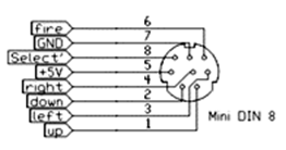
Figure 6
- Joystick Port Connections
|

Figure
7 - Joystick Test Circuit
|
Operation & Test Walkthrough
Install the ROM or insert the
cartridge, connect the loop-back connectors, connect a monitor or correctly
tuned TV and finally the PSU, then power on the machine. Most of the screen
shots that follow are either grabbed from YAPE or VICE simply because the
quality is better, but some of the ones that rely on the loop-backs are taken
with a camera pointing at my LCD TV.
Low Ram Test
The first sequence of tests is
run as soon as the CPU hands over execution to the diagnostic ROM. The
principle is to execute a memory test of the address space of $0002-$0FFF
without making any use of the Zero Page or Stack. This is complicated by the
restriction that we only have the A, X & Y registers available on the CPU
and you also need to have some means of communicating a meaningful status back
to the user in the case of finding a fault. The test routine achieves this by
using the stack pointer (SP) as a fourth register and the screen and border
colour to communicate the status.
First is a data-bus test which
writes a sequence of values to a fixed location, in this case $00FF. The values
test each data line in turn, using values 1,2,4,8 etc. Any failure to read back
the same value will either indicate a problem with the data line or with one of
the DRAMs. I say either because although these tests can give a strong indication
of where the problem may lie, it is frequently impossible to be definitive.
If a problem is detected, the
border will flash from 1 to 8 times, followed by a short pause. The number of
flashes indicates which data line is at fault. Additionally, the screen
background colour is set to red, so you can tell where in the test sequence the
problem was found.
The screen contents are a
useful source of information when diagnosing ram faults; it is possible to
identify stuck data lines or addressing faults just by looking at the screen
contents. For this reason, if the ram tests detect an error and drop into the
screen flash, the screen will alternately fill with ‘@’ symbols and ‘ ’,
which are values $00 and $FF respectively. It will also alternate from filling
top downwards and bottom upwards, to help identify addressing faults. The
patterns you should see are shown below in Screenshot 1 - Low RAM Flash Screens.
’,
which are values $00 and $FF respectively. It will also alternate from filling
top downwards and bottom upwards, to help identify addressing faults. The
patterns you should see are shown below in Screenshot 1 - Low RAM Flash Screens.
If you see the screen filling
with values other than with ‘@’ or ‘’, or the fill is not
uniform, this indicates a RAM problem and you may be able to determine the
problem by cross referencing the observed characters with Table 3. Note that
the CBM characters do not render correctly on the web page. As there would
be no point proceeding with any further tests if the zero page or stack is at
fault, the machine will continually repeat the flash cycle until powered off or
reset.
Screenshot
1 - Low RAM Flash Screens
Symptom
|
Cause
|
Symptom
|
Cause
|
Plus/4 IC
|
C16/C116 IC
|
|
A instead of @
|
D0 stuck high
|
instead of
|
D0 stuck low
|
U11
|
U5
|
|
B instead of @
|
D1 stuck high
|
instead of
|
D1 stuck low
|
U12
|
U5
|
|
D instead of @
|
D2 stuck high
|
instead of
|
D2 stuck low
|
U13
|
U5
|
|
H instead of @
|
D3 stuck high
|
instead of
|
D3 stuck low
|
U14
|
U5
|
|
P instead of @
|
D4 stuck high
|
instead of
|
D4 stuck low
|
U15
|
U6
|
|
(space) instead of @
|
D5 stuck high
|
instead of
|
D5 stuck low
|
U16
|
U6
|
|
instead of @
|
D6 stuck high
|
instead of
|
D6 stuck low
|
U17
|
U6
|
|
instead of @
|
D7 stuck high
|
instead of
|
D7 stuck low
|
U18
|
U6
|
Table
3 - Low RAM Flash Screens (does not display on web page, download PDF)
The second low-RAM test is
designed to identify addressing faults. The RAM tests implemented in the
original Commodore diagnostic tools wrote the same byte across the entire
address space. This makes them unable to highlight addressing related issues,
such as failed multiplexers.
The address bus testing in
Diag264 tries to be a bit smarter. It implements a more elegant test which
writes a bit pattern to a given memory address, and then writes the inversion
of this bit pattern to all the complementary addresses where the address
differs by the inversion of only one of the address bus lines.
In Diag264 we use a base
address at $00FF, so we first write $00 to the addresses in Table
4, which are $00FF plus all the complementary addresses of $00FF below $0FFF.
Then we write a value of $FF only
to $00FF, and check that all of the other addresses still contain $00. If there
is any problem decoding addresses, or there is a stuck address lines in either
in the multiplexers or the RAM’s themselves, then one or more of the addresses
above would also appear to have changed. This is a simple but powerful tool to
detect addressing problems.
Faults are reported using the
same mechanism as the data-bus test, except the background will be blue. The
number of flashes corresponds to the address line where the problem was
identified, as shown in Table 4. As before, further clues may be determined by
observing the screen contents during the screen flash cycles. Problems found in
the addressing tests often indicate failed multiplexers (74LS257) which are in
positions U7 and U8 on a C16/C116 and U9 and U10 in a Plus/4.
|
Address
|
Address
Bus
|
Flashes
on failure
|
|
$007F
|
0000 0111
1111
|
8
|
|
$00BF
|
0000 1011
1111
|
7
|
|
$00DF
|
0000 1101
1111
|
6
|
|
$00EF
|
0000 1110
1111
|
5
|
|
$00F7
|
0000 1111
0111
|
4
|
|
$00FB
|
0000 1111
1011
|
3
|
|
$00FD
|
0000 1111
1101
|
2
|
|
$00FE
|
0000 1111
1110
|
1
|
|
$00FF
|
0000 1111
1111
|
base address
|
|
$01FF
|
0001 1111
1111
|
9
|
|
$02FF
|
0010 1111
1111
|
10
|
|
$04FF
|
0100 1111
1111
|
11
|
|
$08FF
|
1000 1111
1111
|
12
|
Table
4 - Address Bus Flash Codes
The final low-ram test is a
device test, which writes a sequence of 20 test bytes across the address,
followed by a pseudo random pattern. The bytes are:
$7F, $BF, $DF, $EF, $F7, $FB,
$FD, $FE, $80, $40, $20, $10, $08, $04, $02, $01, $FF, $AA, $55, $00
The screen border will cycle
through a sequence of colours as each test byte is used and, as the low-ram
area includes the screen and colour memory, you will see the contents of the
screen rapidly change. The same reporting mechanism of flashing the border is
used if an error is found during this test, with the screen background being
black. If a failure occurs at this point, the number of screen flashes will
point very strongly to the defective DRAM. The table below shows which IC is
the likely problem.
|
Flashes
|
Bit
|
Plus/4
IC
|
C16/C116
IC
|
|
1
|
D0
|
U11
|
U5
|
|
2
|
D1
|
U12
|
U5
|
|
3
|
D2
|
U13
|
U5
|
|
4
|
D3
|
U14
|
U5
|
|
5
|
D4
|
U15
|
U6
|
|
6
|
D5
|
U16
|
U6
|
|
7
|
D6
|
U17
|
U6
|
|
8
|
D7
|
U18
|
U6
|
Table 5
- Possible Failed RAM Chips
Once in the flash sequence,
problems with particular devices will often be visually obvious as the screen contents
cycle between $00 and $FF. For example, if on a Plus/4 U15 has failed leaving
bit 4 stuck high, instead of seeing alternating ‘@’ and ‘’ symbols, you would see ‘P’
(hex value $10) and ‘’.
Once the low RAM tests have
completed, Diag264 knows that the zero-page and stack are now functioning
correctly, so the stack is initialised and the TED registers set up as they
would be on normal machine start-up. As we now know the screen RAM is
functional, we can revert to a more human friendly form of communication before
moving on to the more comprehensive tests.
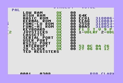
Screen Layout
Now is a good time to explain the general layout of the
screen, most of which is self-explanatory. Look at the screenshot of a
completed test cycle in Screenshot 2. On the top line is the Diag264 web page
link. On the bottom line, from left to right, is the current cycle number in
hexadecimal, the current random number seed used in the RAM tests, and the
video mode. In the bottom right corner is my name and the year, and below is
the release version and build number. The build number is the timestamp of when
the binary was compiled, in the format YYYYMMDDHHMM.
Down the left side is the name of current test in progress,
followed by the status of the completed tests, which would be OK, FAIL, or
SKIP. The next numeric column is the total number of failures for this test
since the tests started. If the diagnostic is left on continuous loop, this is
useful for spotting intermittent failures. To the right is information specific
to the test, which is covered in the explanations below. As each test runs, the
cursor will flash to the immediate right of the test name. The area below the
list of tests may contain various other additional information, depending on
the current test.
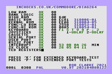
Screenshot
2 - Screen Layout
Bank logic Test
The Bank Logic test serves two
purposes; to test the “Enable RAM” virtual TED register at $FF3E, and then to
test the ROM selection logic implemented by writing to address locations
$FDD0-$FDDF. The first test sets the $FF3E register then checks to see if RAM
is visible in the kernal area. If this fails, you will see something like Screenshot 3 – Enable RAM Failure, with a brief description in a message box.
Problems with this register would usually indicate a problem with the TED chip.
The second test compares a
sequence of bytes in various ROM configurations, ensuring that the expected
bytes are visible as the low-ROM and high-ROM configurations are switched. This
test can identify three possible failure conditions. Firstly that the low-ROM
banking is not switching as expected, then that the high-ROM banking is not
switching, and finally that the kernal does not always remain visible in the
area from $FC00 to $FCFF. In the 264 architecture, the kernal banking routines
reside in this area and the PLA has logic to ensure that that the kernal is
always visible, irrespective of which high-ROM bank is selected. In Screenshot 4 – ROM Banking Failure all three messages are shown as an example, but
only those detected will be displayed during normal operation.
The banking logic is controlled
by the PLA and three supporting logic chips. The locations are shown below in Table 6 - Banking Logic Chips. If Diag264 does highlight an issue with the ROM
banking logic, any of the below chips could potentially be at fault.
|
Chip
|
Plus/4
|
C
16
|
C116
|
|
PLA 251641-02
|
U19
|
U16
|
U101
|
|
74LS139
|
U20
|
U14
|
U103
|
|
74LS175
|
U21
|
U15
|
U105
|
|
74LS27 / 74LS02
|
U22
|
U12
|
U104
|
Table
6 - Banking Logic Chips
The message box will remain visible for approximately 5
seconds before being cleared and moving onto the next test, however the summary
message to the right of the test status will remain visible.
High Ram Test
The high RAM test performs a
similar sequence of tests to the low RAM tests, but on the memory area from
$1000 to the upper end of installed RAM, which could be $3FFF, $7FFF or $FFFF,
depending on the model under test. The test first identifies the amount of
installed RAM by writing a sequence of bytes to $30 and checking to see if they
are mirrored at $4030 or $8030. The amount of installed memory is displayed when
the test completes.
On a 64K system we also need to test the
RAM that resides beneath the ROM’s. To do this, the test code is copied to
$0200 and the RAM made visible by writing to the TED pseudo register at $FF3F.
As it’s not possible to access the RAM beneath the I/O areas, memory is then
tested up to $FCFF and then from $FF20 to $FFFF, skipping locations $FF3E and
$FF3F.
In order to speed the tests up,
the screen is blanked, allowing us to make use of the clock doubling feature of
the TED architecture. On a 64K system they will take approximately 20 seconds
to complete and the screen colour will cycle as the test values change.
Two types of error can be
reported, either an addressing or a device error. The addressing error occurs
when performing the same type of address testing as described in the low RAM
tests, only this time testing the complete address range. As shown in Screenshot 5 - RAM Address Failure the address where the error occurred will be
displayed, as well as an “exclusive or” between the written and expected value.
Additionally, a message box will be displayed for a few seconds highlighting
the chips possibly at fault, which for addressing errors could be the 74LS257
multiplexers. Due to the limitations of testing only via software, this cannot
be definitive, and addressing errors can also come from physical issues on the
PCB and the CPU itself.
A device error occurs when a
value read does not match what was written to a given memory location. As well
as the byte pattern tests as described in the low RAM tests, the high RAM device
test also writes a sequence of pseudo random numbers across the address space
to try and catch subtle pattern memory issues that otherwise would not show up.
If Diag264 is left running, each iteration of the high RAM test will start with
a new seed value, ensuring the maximum possible exercising of the RAM.
As shown in Screenshot
6 – RAM Device Failure the address where the error occurred is again displayed,
as well as an “exclusive or” between the written and expected value. Also, a
message box will be displayed which will attempt to highlight which RAM chip is
likely at fault. The message box lists the chips for the Plus/4, C16, and C116
and does not attempt to guess which machine the tests are running on.
ROM Tests
The ROM tests perform checksums on any installed ROMS,
including those in the Function High and Low sockets in a Plus/4, which would usually
be the 3+1 software. The checksum routine is copied to $0200 in RAM to allow
the different ROM’s to be switched in. The Low ROM area is summed from $8000 -
$BFFF and High ROM from $C000 - $FFFF, with the exception of $FD00 – $FF1F for
the I/O area, the two bytes at $FF3E and $FF3F which are the virtual TED
registers, and for high ROMs other than the kernal, the area from $FC00 - $FCFF
is also skipped as the 264 architecture always exposes the default kernal in
this area to allow the bank switching and interrupt routines to always be
visible.
Each ROM is check summed three times using a cyclic redundancy
algorithm. If an inconsistent value is read, it is assumed no rom is present
and the message ‘SKIP’ is displayed. If SKIP is seen when a ROM is known to be
present, this should be considered a failure. If the checksum of the ROM is
recognised, the part number and revision is displayed. Any other computed
checksum will result in a ‘FAIL’. An example can be seen in Screenshot
7 - ROM Checksum Failure which shows a problem with the ROM in the Function Low
socket.
All known official ROM’s are recognised, along with beta
versions, those with modified Hungarian characters sets, and the kernal
modified by Andrew Challis, to support his 6510 CPU replacement. If the ROM is identified,
it will display the text in Table 7 - Diag264 recognized ROM's below, which in
the case of officially released ROM’s, will be the Commodore part number.
|
Description
|
Checksum
|
Diag 264 Display
|
|
Basic ROM Beta 0119 (19th
January 1984)
|
$F885
|
BETA 0119
|
|
Basic ROM Beta 0203 (3rd
February 1984)
|
$23D5
|
BETA 0203
|
|
Basic ROM Beta 0217 (17th
February 1984)
|
$5031
|
BETA 0217
|
|
Basic ROM Release version
|
$EC81
|
318006-01
|
|
Kernal ROM Beta 0119 (19th
January 1984)
|
$1D45
|
BETA 0119
|
|
Kernal ROM Beta 0203 (3rd
February 1984)
|
$0355
|
BETA 0203
|
|
Kernal ROM Beta 0217 (17th
February 1984)
|
$D17A
|
BETA 0217
|
|
Kernal ROM Beta 0316 (16th
March 1984)
|
$424E
|
BETA 0316
|
|
PAL kernal Revision 1 (EPROM only)
|
$33F0
|
318004-01
|
|
PAL kernal Revision 3
|
$1FC9
|
318004-03
|
|
PAL kernal Revision 4
|
$010D
|
318004-04
|
|
PAL kernal Revision 5
|
$EEA6
|
318004-05
|
|
NTSC kernal Revision 4
|
$5FAD
|
318005-04
|
|
NTSC kernal Revision 5
|
$5CD4
|
318005-05
|
|
Hungarian PAL kernal Revision 1
|
$CAE8
|
318030-01
|
|
Hungarian PAL kernal Revision 2
|
$F3DA
|
318030-02
|
|
PAL 6510 CPU replacement (Rev 5)
|
$E02B
|
6510 PAL V1
|
|
NTSC 6510 CPU replacement (Rev 5)
|
$5259
|
6510 NTSC V1
|
|
3+1 Function Low
|
$2558
|
318053-01
|
|
3+1 Function High
|
$00A5
|
318054-01
|
|
Micro Illustrator
|
$36C2
|
MICRO ILLUS.
|
|
Diag264
|
Varies
|
DIAG264
|
Table
7 - Diag264 recognized ROM's
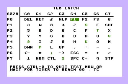
Keyboard Test
The keyboard test checks two aspects of the keyboard operation,
the 6529 single port interface and the keyboard latch on the TED chip. It does
not perform an exhaustive check on the keyboard matrix, as this can be done in
the advanced keyboard tests discussed later. The test can be carried out
manually or by using the keyboard loop-back plugs for unattended testing.
The test first checks to see if the shift-lock is held down.
If so, the remainder of this test, as well as the joystick test, is skipped,
avoiding unnecessary delays waiting for keys that will never be pressed if the loop-back
plugs are not in place. If not, the 6529 keyport is tested to see if it can
hold a value by writing to the port and comparing with the values that are read
back. If any problems are detected with the keyport, the message “6529 KEYPORT
BAD” is shown when the keyboard test completes.
The keyboard port is then cleared (all bits set high) and the
TED keyboard latch sampled. If the latch contains anything other than $FF, this
indicates a possible keyboard problem. At this point a string of 8 keys to be
pressed is displayed on the screen, as seen in Screenshot 8.

Screenshot 8 – Keyboard Test
The test will then pull each of the lines low on the keyport
in turn, keeping each one low for approximately 2 seconds. The leftmost black key
is the one that should be pressed if a keyboard is attached and also
corresponds to the loop-backs on the keyboard connector if that is being used.
The keys and loop-backs have been chosen so that each line on the keyport pulls
a different bit of the TED latch low. If the corresponding bit of the latch
does not go low within two seconds, that port/latch combination is deemed to
have failed, the key is colour red, and the test moves on to the next key.
On success, the key will be coloured green and an additional
test will be done by clearing the port and re-reading the latch register after
a short delay. If the same value cannot be read from the latch it indicates a
problem with the latch being able to hold the value correctly, a common partial
failure of the TED. In this instance the message “TED LATCH BAD” will be
displayed after the joystick test has completed! You can see in Screenshot 8 that the first two keys were successfully detected, 3 and 4 were not,
and the remaining keys are currently being waited for. If a loop-back is being
used the test will complete very quickly if successful.
Joystick Test
The joystick test operates much in the same way as the
keyboard test, except that instead of a list of keys, a list of possible
directions for the two joystick ports is displayed. They will initially be
displayed in black text, which turn green as each direction is detected. The
test does not require the joystick to be actuated in any particular order, and will
be flagged as complete once every direction and fire button has been detected.
If directions are still outstanding after approximately 12 seconds, the test
will be flagged as a fail.
With a suitable loop-back connected, the test will complete almost
instantly. Without a loop-back, the only way to get this to successfully
complete is to have a joystick connected to both of the ports. If you suspect
one of the joystick port has issues but you only have a single joystick, you
should start the test with the joystick on port one, determine that it works or
not, then power off the machine and swap the joystick to the other port.
Although there is some electronic protection on the joystick ports, you
should never swap joysticks over with the power on.
As with the keyboard test, the TED latch is also tested to
determine that it can hold a value. If a latch problem is detected in either
the joystick test or the preceding keyboard test, the message “TED LATCH BAD”
will appear after the test completes. See Screenshot 9.
If a joystick loop-back is not available, activating the shift
lock before the test starts will cause the joystick test to be skipped.
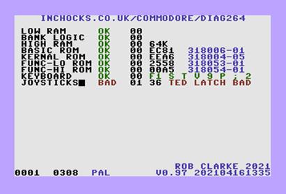
Screenshot
9 - Failed TED Latch
Cassette test
The cassette interface on the 264 series is implemented using
P4, P1, and P3 of the 7501/8501 CPU for read, write, and motor control
respectively. On a Plus/4 the cassette sense is implemented by port bit P2 on
the user port 6529. There is no 6529 on the C16, C116 or C232 but the
equivalent cassette sense operation is mirrored using a tri-state buffer to
drive D2 to the state of the sense line when reading from $FD10.
If the cassette test fails at any point, a status byte will be
shown to the right of the cycle count which will indicate during which step of
the test it failed. The steps in the test are as follows:
01. Start with write low (P1)
and check read (P4) is high.
02. Hold write high and check read
is low.
03. Hold write low and check
read is high again.
04. With the motor off, check if
P7 in unaffected
05. Check P2 of 6529 at $FD10 is
low
06. Turn cassette motor on (P3
low), and check P3 remains low
07. Check P2 of 6529 at $FD10 is
now high.
All of the CPU output ports are inverted by a 7406 at U6 on a
Plus/4 and U9 on a C16/C116. Assuming the loop-back is installed correctly, any
failure in steps 1-6 strongly indicates that either the CPU or the 7406 is
faulty. If a failure occurs at step 7, it implies the cassette sense circuit is
at fault or, more likely, that the circuitry that provide power to the cassette
motor is at fault.
Further diagnosis of the CPU’s I/O ports can be done using the
Advanced Port Testing feature described later.
Serial test
The IEC serial port is internally looped back, with the
exception of the ATN line, which is looped back to CLK in in the connector. As
with the cassette test, a status byte will be shown to the right of the cycle
count which will indicate exactly which step of the test failed. The steps in
the test are as follows:
01. Start with DATA out (P0),
CLK out (P1) and ATN (P2) low and check DATA in (P7) and CLK in (P6) are high.
02. Hold DATA out high and check
DATA in is low.
03. Hold DATA out low and check
DATA in is high again.
04. Hold CLK out high and check
CLK in is low.
05. Hold CLK out low and check
CLK in is high again.
06. Hold ATN out high and check
CLK in is low.
07. Hold ATN out low and check
CLK in is high again.
The serial port shares much of the circuitry with the
cassette, so any problems with this test strongly indicate an issue with the
CPU ports or the 7406 inverter. Again, further diagnosis of the CPU’s I/O ports
can be done using the Advanced Port Testing feature described later.
User Port Test
The user port is only present on the Plus/4 and contains two
interfaces, the 6529 single port interface and the 6551 ACIA RS232 interface. This
test exercises both to determine correct operation, starting with the 6529
port.
After setting all port bits high (inactive), the port is read
over a period of time to ensure the value is stable. This is a best endeavour
to ensure the port is present on the machine being tested, such as a C16, as
the data lines usually float with random values if not. The test will say
‘SKIP’ if it can’t be found. If you know the port to be present, this should be
read as a fail.
The individual data lines of the port are activated in
sequence to ensure they pull the corresponding looped back data line low (see Figure 4) if not, the test will fail. In this instance, the status byte will contain
the hexadecimal representation of the failed port bits. The Advanced Port
Testing also allows you to directly manipulate the state of the port bits for
further analysis.
RS232 Port test
The ACIA is rather more complex to test as the communication
is interrupt driven. First an interrupt handler is set up in the low memory
error to catch the communication related interrupts and then the port is
configured for 8-bit words, 1 stop bit, and 2400 baud. If this value cannot be
read back from the control register, the ACIA port is assumed not to be present
and skipped. If any of the following steps fail, the step will be indicated in
the status byte.
01. RTS and DTR
are cleared. DSR is checked to see if it is set.
02. DCD is
checked to see if it is set.
03. Interrupts
are enabled and DTR is set ready. After a short delay, check that an interrupt
has occurred and that DCD has been cleared.
04. RTS is set
ready. After a short delay, check that an interrupt has occurred and that DSR
has been cleared.
Now a sequence of 192 test bytes is set up and transmitted
using the ACIA. All the communication is interrupt based, interrupts being
generated when the receive register (all 1 byte of it) is full and when the
send register is empty. The location for the received message is set up to be
about ¾ of the way down the screen, so if the message is received correctly,
you should see something like Screenshot 10.

Screenshot
10 - RS232 Test
The test waits approximately 2.5 seconds for the message to be
received before checking the following conditions have been met.
05. Check that ‘bytes to send’
is now zero.
06. Check that ‘bytes received’
is now 192.
07. Check no overflow errors
occurred.
08. Check no framing errors
occurred.
09. Check no parity errors
occurred.
10. Check the contents of the
receive buffer match the send buffer
Interrupt & 2X Clock Tests
The interrupt tests check that the interrupt sources on the
TED chip are all functioning correctly. The TED has 4 usable interrupt sources;
3 timers and the raster interrupt. These are initialised to a specific
pre-condition and then allowed to run for approximately half a second, counting
the number of interrupts that occurred. If this number falls outside of the
boundaries shown below, the TED may be at fault.
The number of triggered interrupts during the period is
affected by the video standard of the machine under test (different number of
lines to render) as well as the presence of an ACIA on the system (causes more
interrupts).
The test is performed twice, the first time with the TED
forced into single clock mode and the second time with the screen blanked, thus
running at twice the speed. The interrupt sources and the boundaries currently
defined for both single and double clock operation are seen in Table 8 - Interrupt Sources and Boundaries.
|
|
Single Clock
|
Double Clock
|
|
Interrupt Source
|
Lower Bound
|
Upper Bound
|
Lower Bound
|
Upper Bound
|
|
Timer 1 with a
reload value of $2000
|
$53
|
$56
|
$26
|
$26
|
|
Timer 2,
initialised with $0100
|
$0B
|
$0B
|
$05
|
$05
|
|
Timer 3,
initialised with $FF00
|
$0A
|
$0A
|
$04
|
$04
|
|
Raster
Interrupts at scan line 204
|
$26
|
$2E
|
$11
|
$14
|
Table
8 - Interrupt Sources and Boundaries
Each count will be displayed as it completes; in green if
within the boundaries defined above, otherwise red. An example of the output
for a successfully completed test is shown in Screenshot 2, earlier in the
document.
Upon completion of all tests, the number of detected
interrupts will cycle between the minimum and maximum values while Diag264
pauses at the end of each cycle. If any of the counts do vary, they will flash
blue.
TED Register Tests
The final sequence of tests attempts to test as many of the
TED registers as can reasonably be achieved in a short space of time. Some of
the registers have already been tested prior to this section, for example the
screen blanking, clock doubling and timers. For most of the remaining registers
it is not possible for the software to determine an ‘OK’ or ‘FAIL’ state so it
relies on the observer to make that decision after comparing the results to
this document.
A sequence of three screens is displayed, and the observer
should be on the lookout for deviations from what is described and shown below.
A musical scale is played for the duration of each screen using one of the
three voices for each of the screens.
Colour Palette
This screen plays a scale on voice 1
and displays a cycling colour palette. It doesn’t really do much more than show
off the TED’s colour palette.

Screenshot 11
- Colour Palette
TED Graphic Modes
The second screen has much more going on and is designed to
show the available graphics modes on a single screen using raster interrupts to
change the mode between sections. You should check carefully that what is shown
on the screen matches Screenshot 12 - TED Graphics Modes. The modes displayed
are shown alongside the screenshot. There should be no observable flickering or
other artefacts on the screen.
The top three sections show the three different text modes.
Each section shows four rows of characters with tile values of 0 – 39, 64 –
103, 128 – 167 and 192 – 231 respectively. The attribute (colour) values are
set to the same value.
The first, with the dark blue border is the default Hi-Res
text mode. Although not seen in the static picture, the third and fourth rows
will be flashing. The second, with the black background, shows multicolour
mode, which is not really suited to the inbuilt character set but should
nevertheless be noticeable on characters 8 – 15 and 24 – 31. The third text
mode, with the yellow background, shows the rarely used extended background
mode, where the first 64 characters are rendered on a different coloured
background depending on the value of bits 6 and 7 of the tile value.
The bottom two sections highlight the bitmap graphics modes,
Hi-Res and multicolour, with respective green and red borders. The top should
show a grid of white lines and the bottom a grid of alternating vertical blue
and red lines with green horizontal lines.
|

Screenshot 12 - TED Graphics Modes
|
Top Border
|
|
Hi-Res Text
|
|
Multicolour Text
|
|
Extended Background
Text
|
|
Hi-Res Bitmap
|
|
Multicolour Bitmap
|
|
Bottom Border
|
|
|
Smooth Scroll
The final TED register test demonstrates the smooth scrolling
and the 24 row, 38 column modes. The status screen is moved in a sinusoidal
wave. There should be no visible artefacts on any of the borders or any
shearing of the display. The white noise generator should be heard during this
test.
Screenshot 13
– Smooth Scroll
Test Cycle Completion
At the end of the test, the display will pause for a few
seconds before looping round and continuing from the High RAM test again.
During this time, the minimum and maximum interrupt values will be displayed,
if any. You also have the option to select from two advanced tests, pressing
‘K’ for the extended keyboard tests, and ‘P’ for the extended ports testing. If
the keyboard loop-back plug is detected, this option will not appear, as
clearly the keyboard is unavailable.
Just before starting again, a brief sample will play to test
the TED’s digital sample playing capabilities.
Extended Keyboard test
When the main tests complete, there will be a pause of a few
seconds before the cycle starts again.
The advanced keyboard tests were implemented to identify
keyboard reliability issues and to identify patterns which may cause complete
rows or columns of keys to fail, which may in turn indicate that there is a
problem with the keyboard output port or TED latch. Fundamental problems should
be detected by the man keyboard test, but this allows for an additional level
of investigation.
Displayed you will see a screen as shown in Screenshot
14 – Advanced Keyboard Testing, which shows the keyboard not as it is
physically laid out, but according to the rows and columns of the 6529 keyboard
port and TED latch. Initially, all keys will be black, showing that the key has
not yet been pressed. While each key is pressed, it will highlight in a
reversed green colour, which will revert to non-inverted, but still green, once
the key is released.
Using this, you can go through all keys ensuring that they are
responding correctly, including when used in conjunction with either shift, shift-lock,
or the Commodore key.
Screenshot
14 – Advanced Keyboard Testing
To exit the keyboard test, either press ‘Control’ and ‘Q’, or
wait for the hexadecimal countdown timer to reach 00, after which the main test
cycle will restart.
Extended Port tests
The extended port testing functionality was added to enable
more detailed investigation of the I/O ports on the CPU and, if fitted, the
6529 on the user port. Having issues with the ports can cause problems with the
cassette deck and the IEC port for disk drives and printers. As well as the CPU
itself, some of the failure points include the 7406 hex inverter and the diodes
that protect the I/O lines. During normal operation, it can be quite difficult
to investigate these without an oscilloscope as the states change very quickly,
but this tool allows you to maintain the ports in a steady state and toggle them
as required.
After the pressing ‘P’, you will see an image similar to the
one shown in Screenshot 15 – Extended Ports Testing . At the top of the screen
is the CPU with the CPU DDR (Data Direction Register) at memory location $00,
followed by the write value to the CPU port register itself at location $01,
and finally the value read back from the port register. All the values are
shown as a hexadecimal value, followed by a binary representation of the
register. For the DDR these are represented by ‘I’ and ‘O’ for Input and Output
respectively. For the written value, port bits set to input by the respective
value in the DDR are displayed as a dash ‘-‘, and ports set to output displayed
as a solid block for a high value, and a dot ‘.’ for a low value. For the read
value, the same scheme applies, again being shown as a solid block for a high
value and a dot for a low value. To the right is a summary of the use of the
CPU port on 264 computers.
Below the CPU is the 6529 SPI (Single Port Interface) at
location $FD10 which is exposed on the user port of the Plus/4. The 6529 does
not have a corresponding DDR, so just the write and read values are shown. To
the right is shown the only standard use of this port, where P2 is used for
cassette sense. On a C16, the 6529 is not present, but the ability to read P2
is still implemented using some basic TTL logic.

Screenshot
15 – Extended Ports Testing
Operation is quite simple, in that the ‘CTRL’ key is used to
rotate between the CPU DDR, the CPU port write value and the 6529 write value. The
selected port is highlighted in reversed green text. Once selected the
individual register bits are manipulated using the keys ‘0’ to ‘7’. On the DDR,
these will toggle the port bits between input and output, while on the write
values this will toggle between high and low outputs.
On the CPU port, any bits set as input via the DDR cannot be
changed. The default value for the DDR on 264 machine is $0F, meaning port bits
0 to 3 are outputs and 4 to 7 are inputs. There should not normally be any
reason to change the DDR from its default value, as once set by the kernel, it
is never changes during the normal operation of the machine and neither does
any other software change it to my knowledge.
If you have a cassette deck attached, then pressing play, fast
forward, or rewind, should cause the cassette sense bit to toggle. Toggling P3
on the CPU output will cause the motor to start and stop. With the motor
enabled, playing a tape with a program on should cause P4 to flicker rapidly.
As some of the CPU ports are internally connected, then
without the loop-back plugs installed toggling P0 should affect the input on
P7, and likewise P1 will affect P6.
If you have the loop-back plugs installed, then P3 (motor)
should toggle the sense line, and P1 (cassette write) should toggle P4
(cassette read.)
DIAG264 Version History
0.15A -
added colour to print_msg
-
made sure that keyport and latch messages are always displayed
-
fixed long standing bug with timer 3 checks
0.20A -
re-write of rom check routine
0.21A -
updated ZP usage
0.22A -
tidied low-ram test, integrated ted mode screen
0.4A -
integrated smooth scroll
-
added databus and address bus tests
-
added 128 char definitions
0.5A -
added better address bus tests and for high ram
0.6A -
added HW cursor
0.7A -
tolerance checks on interrupt counts
0.1B -
High RAM location reporting
-
fixed a raster synch issue with the interrupt counts which should improve count
stability
-
implemented NTSC compatible tests...
0.11B -
allowed skipping of KB test even if failures have occured
0.12B -
improved latch testing on KB test
0.13B -
fixed keyport bug
-
fixed setting of cassette motor if sense is on cpu-p7 so it doesn't break
serial test
-
fixed location of $FD10-D2 message
0.2B -
first Beta release!
-
relaxed interrupt tolerances based on running on NTSC machine
0.3b -
much improved address bus test
0.5b -
fixed databus test to correctly mask bits
0.6b -
Autodetect PAL/NTSC if running from cartridge (F33F - #$08 for PAL, #$48 for
NTSC)
-
Always allow KB skip
0.7b -
Fixed NTSC/PAL toggle. 'P' forces PAL and 'N' forces NTSC
-
Avoid conflict if dongle installed
0.8 -
Updated version & 2016
-
remove cpu-p7 cassette checks, messages etc
-
fixed raster detection in colour_sound_test
-
simplified colour sound test
0.9 -
Updated version & 2018
-
ROM checksums now CRC-16
-
use a single smooth scroll dataset and manipulate bits
-
various minor code optimisations
-
Doesn't trash the screen when check-summing function ROM's
-
stabilised raster splits
-
added various beta kernals
0.91 -
added extended KB test
-
fixed small bug in forcing NTSC mode
-
cart version now works in any low-rom position, including replacing func-low
-
cart_lo renamed to low_rom
-
fixed bug caused by small_delay sitting across a page boundary causing interrupt…
- …timing discrepancies
-
align interrupt handler to page boundary, again to avoid timing discrepancies
-
added pseudo random number testing to RAM
0.92 -
added advanced port testing
-
added checksum for Andy Challis' 6510 replacement kernal
-
reset interrupt sources at end of TED interrupt tests
0.93 -
beta release
-
changed keys to toggle ports to 0->7 instead of 1->8
-
Added some information to the EPT tests to describe the use of the ports
-
reset the ports at the beginning of EPT
-
show Diag264 and not FAIL if running from low-ROM socket
0.94 -
fixed bug that always sent the tests into the port testing if the KB loop-back
plug…
- …was installed
- added check to detect KB dongle and if present
don't show messages for advanced tests
0.95 -
updated to 2020
- fixed small bug which compared 3 bytes instead of
2 when comparing ROM CRC checksums.
A legacy from the old 3 byte checksum.
0.96 -
make TED mode use raster interrupts
- simplified tune playing routine
- reduce time waiting for joystick input, reduced to
#$c0
- improve error reporting on joystick test. (Alex
Korth email May 2019)
- if the latch doesn't have correct value at start,
or is unstable during reading, print
as status byte
- pop up a message box on ram failures suggesting
chip at fault
- fixed bug where using shift-lock to skip keyboard
and joystick persisted for joystick
on subsequent cycles
- moved receive buffer up a bit to make look neater
- reviewed and updated ZP usage
- added new banking logic tests for FF3E and FDD0
- added error for unexpected interrupts
- play a Homer Simpson WooHoo! sammple at the end of
each test cycle
- added exomizer decompression for sample data an
other stuff for future
- added Andy Challis NTSC kernal for 6510 adapter
- stabilise the interrupt counts by refactoring int
handler, skip false ACIA IRQ's if
not present
- display min and max interrupt counts, highlighting
differences at end of cycle
- explicitly set raster line on interrupt tests to
204, previously set by TED defaults
- updated to 2021
|

Figure 8
- Shady Cat
|